- 您现在的位置:买卖IC网 > Sheet目录1889 > AD5200BRMZ50-REEL7 (Analog Devices Inc)IC POT DGTL 50K 256POS 10MSOP
–4–
AD5200/AD5201–SPECIFICATIONS
ELECTRICAL CHARACTERISTICS
Parameter
Symbol
Conditions
Min
Typ
1
Max
Unit
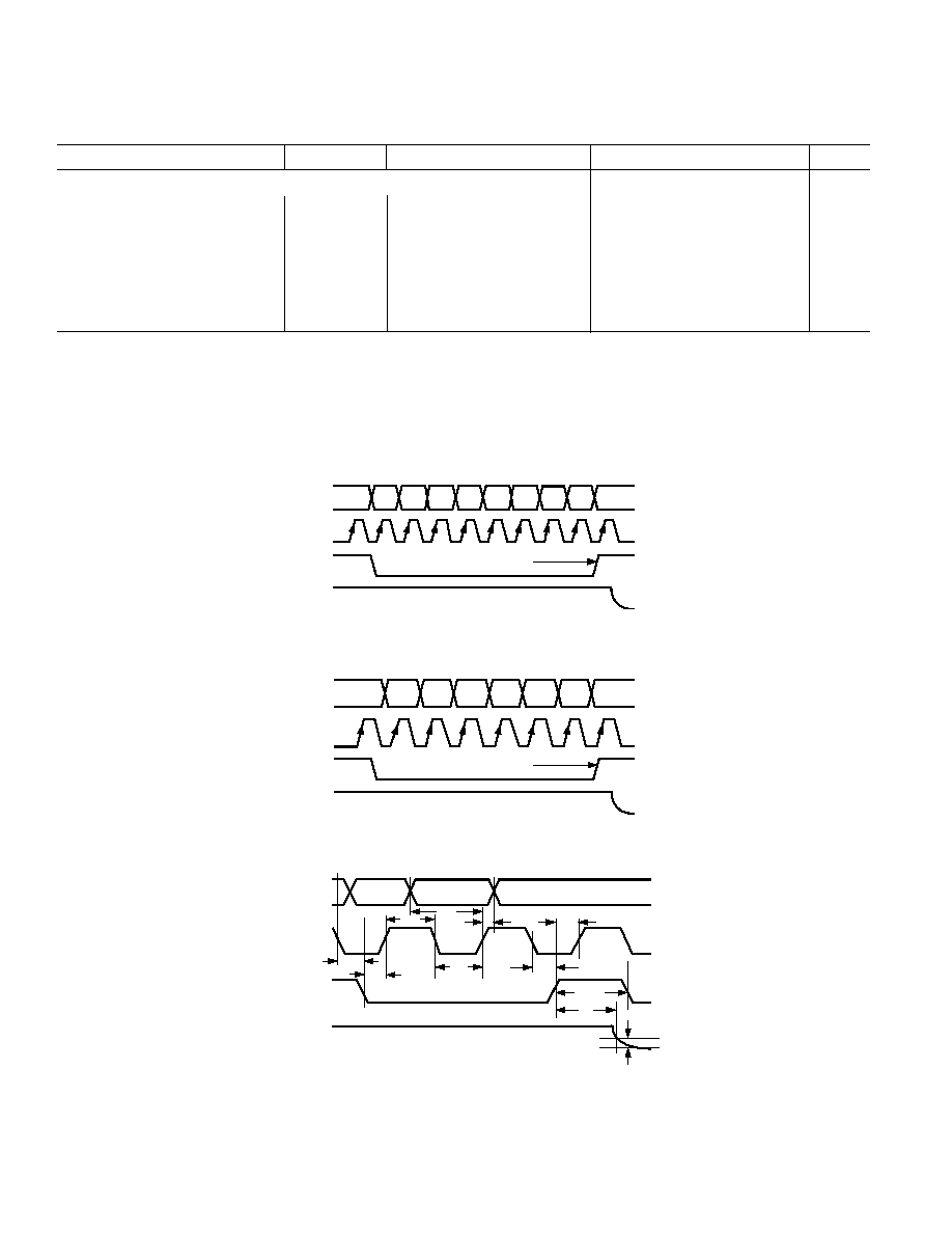
INTERFACE TIMING CHARACTERISTICS (Applies to All Parts [Notes 2, 3])
Input Clock Pulsewidth
tCH, tCL
Clock Level High or Low
20
ns
Data Setup Time
tDS
5ns
Data Hold Time
tDH
5ns
CS Setup Time
tCSS
15
ns
CS High Pulsewidth
tCSW
40
ns
CLK Fall to
CS Fall Hold Time
tCSH0
0ns
CLK Fall to
CS Rise Hold Time
tCSH1
0ns
CS Rise to Clock Rise Setup
tCS1
10
ns
NOTES
1Typicals represent average readings at 25
°C and V
DD = 5 V, VSS = 0 V.
2Guaranteed by design and not subject to production test.
3See timing diagram for location of measured values. All input control voltages are specified with t
R = tF = 2 ns (10% to 90% of 3 V) and timed from a voltage level of
1.5 V. Switching characteristics are measured using VLOGIC = 5 V.
Specifications subject to change without notice.
(VDD = 5 V
10%, or 3 V
10%, VSS = 0 V, VA = +VDD, VB = 0 V, –40 C < TA < +85 C
unless otherwise noted.)
D7
D6
D5
D4
D3
D2
D1
D0
0
1
SDI
0
1
CLK
0
1
VOUT
0
1
CS
DAC REGISTER LOAD
Figure 1a. AD5200 Timing Diagram
0
1
SDI
D5
D4D3
D2D1
D0
0
1
CLK
0
1
CS
DAC REGISTER LOAD
0
1
VOUT
Figure 1b. AD5201 Timing Diagram
Dx
0
1
0
1
0
1
0
VDD
SDI
(DATA IN)
CLK
CS
VOUT
t
CH
t
DS
t
DH
t
CS1
t
CSW
t
S
t
CL
t
CSH0
t
CSS
1LSB
t
CSH1
Figure 1c. Detail Timing Diagram
发布紧急采购,3分钟左右您将得到回复。
相关PDF资料
AD5203ARZ100
IC POT DGTL QUAD 64POS 24SOIC
AD5204BRZ50
IC DGTL POT QUAD 50K 24-SOIC
AD5207BRU50
IC DGTL POT DUAL 256POS 14TSSOP
AD5220BNZ50
IC POT DGTL SGL 128POS 8DIP
AD5222BRUZ100
IC POT DGTL DUAL 128POS 14TSSOP
AD5227BUJZ10-R2
IC DGTL POT 10K UP/DN TSOT23-8
AD5228BUJZ50-R2
IC DGTL POT 50K UP/DN TSOT23-8
AD5231BRU50-REEL7
IC DGTL POT 1024POS 16-TSSOP TR
相关代理商/技术参数
AD5201
制造商:AD 制造商全称:Analog Devices 功能描述:256-Position and 33-Position Digital Potentiometers
AD5201BD
制造商:Rochester Electronics LLC 功能描述:- Bulk 制造商:Analog Devices 功能描述:
AD5201BRM10-REEL7
制造商:Rochester Electronics LLC 功能描述:5-BIT DIGITAL POT - Tape and Reel 制造商:Analog Devices 功能描述:
AD5201BRM50
制造商:Analog Devices 功能描述:Digital Potentiometer 33POS 50KOhm Single 10-Pin MSOP 制造商:Rochester Electronics LLC 功能描述:5-BIT DIGITAL POT - Bulk
AD5201BRM50-REEL7
制造商:Analog Devices 功能描述:Digital Potentiometer 33POS 50KOhm Single 10-Pin MSOP T/R 制造商:Rochester Electronics LLC 功能描述:5-BIT DIGITAL POT - Tape and Reel
AD5201BRMZ10
功能描述:IC DGTL POT 10K 33POS 10-MSOP RoHS:是 类别:集成电路 (IC) >> 数据采集 - 数字电位器 系列:- 标准包装:3,300 系列:WiperLock™ 接片:257 电阻(欧姆):100k 电路数:1 温度系数:标准值 150 ppm/°C 存储器类型:易失 接口:3 线 SPI(芯片选择) 电源电压:1.8 V ~ 5.5 V 工作温度:-40°C ~ 125°C 安装类型:表面贴装 封装/外壳:8-VDFN 裸露焊盘 供应商设备封装:8-DFN-EP(3x3) 包装:带卷 (TR)
AD5201BRMZ10-REEL7
功能描述:IC DGTL POT 10K 33POS 10-MSOP RoHS:是 类别:集成电路 (IC) >> 数据采集 - 数字电位器 系列:- 标准包装:3,000 系列:DPP 接片:32 电阻(欧姆):10k 电路数:1 温度系数:标准值 300 ppm/°C 存储器类型:非易失 接口:3 线串行(芯片选择,递增,增/减) 电源电压:2.5 V ~ 6 V 工作温度:-40°C ~ 85°C 安装类型:表面贴装 封装/外壳:8-WFDFN 裸露焊盘 供应商设备封装:8-TDFN(2x3) 包装:带卷 (TR)
AD5201BRMZ50
功能描述:IC DGTL POT 50K 33POS 10-MSOP RoHS:是 类别:集成电路 (IC) >> 数据采集 - 数字电位器 系列:- 标准包装:3,300 系列:WiperLock™ 接片:257 电阻(欧姆):100k 电路数:1 温度系数:标准值 150 ppm/°C 存储器类型:易失 接口:3 线 SPI(芯片选择) 电源电压:1.8 V ~ 5.5 V 工作温度:-40°C ~ 125°C 安装类型:表面贴装 封装/外壳:8-VDFN 裸露焊盘 供应商设备封装:8-DFN-EP(3x3) 包装:带卷 (TR)